Mos Metaloxidesemiconductor Physics And Technology Ehnicollian Jrbrewspdf Hot
The simplest MOS device is a capacitor: a metal plate (the gate), an insulating oxide layer (typically SiO₂), and a semiconductor substrate (usually silicon). In an ideal MOS capacitor, we assume:
A perfect atomic transition between silicon and silicon dioxide is impossible. Random, unbonded silicon atoms (dangling bonds) occur at the boundary. Nicollian and Brews classified these defects into distinct categories: Interface Traps ( Nitcap N sub i t end-sub
In each of these cases—from the first hot carrier injection studies to the design of a 2 nm GAA transistor—engineers and scientists are using the fundamental framework of MOS physics and technology that E.H. Nicollian and J.R. Brews so masterfully documented.
The book covers the theoretical and experimental foundations of measuring and controlling the electrical properties of the MOS system. Google Books MOS Capacitor Fundamentals
The original 1982 edition (ISBN 0-471-08500-6) was followed by a Wiley Classics Library edition in 2003 (ISBN 9780471430797), a testament to the book's enduring relevance. For decades, it has been an indispensable resource for device physicists, process engineers, and graduate students, often referred to simply as "Nicollian and Brews." The simplest MOS device is a capacitor: a
Starting at the 45 nm node (Intel, 2007), HfO₂ (κ ~25) replaced SiO₂ (κ ~3.9). To avoid phonon scattering and Fermi level pinning, metal gates replaced polysilicon. HKMG enables thicker physical oxide while maintaining equivalent electrical thickness (EOT), drastically reducing leakage.
Here is a comprehensive breakdown of the core physics, measurement technologies, and enduring legacy of this seminal work. 1. The Core Physics of the MOS Capacitor
An alternating current (AC) signal is superimposed on a direct current (DC) bias. As the AC signal fluctuates, interface traps exchange electrons or holes with the semiconductor. This trapping and detrapping process consumes energy, which manifests as an electrical conductance (
: There are primarily two types of MOS transistors: Nicollian and Brews classified these defects into distinct
) is applied, the gate repels the mobile holes away from the interface. This leaves behind fixed, negatively charged acceptor ions, creating a "depletion region" devoid of mobile carriers.
Before examining a fully functional MOSFET, engineers must master the MOS capacitor. This two-terminal device consists of a metallic gate, an insulating oxide layer (historically silicon dioxide, SiO2SiO sub 2 ), and a semiconductor substrate (typically silicon).
C-V Characterization: The primary diagnostic tool for assessing whether a fabrication run was successful.
The Foundation of Modern Electronics: A Deep Dive into MOS Physics and Technology The book covers the theoretical and experimental foundations
Phenomena like Bias Temperature Instability (BTI) and Hot Carrier Injection (HCI) are rooted in the dynamics of charge trapping at oxide boundaries. Understanding the kinetics of these traps requires the precise thermodynamic and statistical mechanics outlined in this classic text. 5. Conclusion
The MOS transistor is the most manufactured human artifact in history. Whether you are debugging a 28nm planar chip or designing a 2nm GAA device, the physics doesn't change: it’s about controlling the gate, protecting the oxide, and mitigating the hot carriers.
This injection process has several detrimental effects:
) and oxide charges. In an ideal world, the interface between silicon and silicon dioxide is perfectly clean. In reality, dangling bonds and chemical impurities create localized energy states within the silicon bandgap.
) that form the basis for SPICE transistor modeling still used by circuit designers today. 4. Modern Relevance: High-k/Metal Gates and FinFETs
The text is structured to take a reader from the basic principles to advanced, analytical measurement techniques. 1. The MOS Capacitor Mechanism
Mos Metaloxidesemiconductor Physics And Technology Ehnicollian Jrbrewspdf Hot
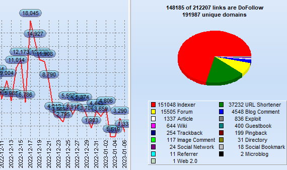
What exactly is GSA SER Verified List? And What is the best way to rank on It?
GSA Search Engine Ranker (SER) is an effective tool utilized by SEO professionals to create high-quality
link opportunity for their websites.
With GSA SER, marketers are able to quickly develop an inventory of verified hyperlinks that are
specifically tailored to the specific requirements of their clients. This allows them to concentrate on
those that are relevant and achieve the most effective outcomes.
Benefits of Using a GSA SER Verified List
The use of the GSA verified list for SER enables marketers to quickly and effortlessly identify top-quality
link building opportunities that can improve their rankings on search engine result page (SERPs).
It is constantly updated continuously to ensure that marketers can be assured that they are receiving the
most recent information available. Furthermore, many of the websites listed on the list are from sites that
are low-OBL Tier 1 This means they are more likely to attract high traffic and aid your blog or website to
climb up the ranks.
How Do You Improve Your Ranking by using the help of a GSA Verified Lists of SERs?
Once you've found opportunities to build links from the GSA SER verified list, it's crucial to concentrate
on creating content of high quality that is engaging for users and ultimately get them clicking on your site
or blog.
Making informative, useful and relevant content can help you get higher rankings on the results pages of
search engines by demonstrating to Google that your website is an authority in the topic. It is also
important to ensure that all links link back to your site or blog, since this will provide Google the
impression of trustworthiness and relevancy when it comes to ranking.
What Are Some Best Practices When Using a GSA SER Verified List?
If you are using a GSA SER verified list, bear in your mind that when you are looking at link opportunities
for building quality must always take priority over the quantity. In addition, focusing on generating
articles that are valuable to users rather than trying to build the most links possible will ensure higher
rankings in the long run.
Not last, you should be careful not to overuse keywords overly often to prevent your website from being
considered low-quality or spam and causing your rankings to drop instead of increasing.
Conclusion: SER Verified List
Utilizing the GSA SER list will offer SEO professionals with top-quality link
building options specifically to their requirements that can result in better rankings for their site or
blog over time, if followed correctly, following best practices, such by focusing on the creation of
high-quality content, not quantity, as well as avoiding keyword stuffing and so on.
In the end making use of this tool in the right way will allow you to achieve higher results in search
engine optimization more quickly than ever before!
Order Now
The simplest MOS device is a capacitor: a metal plate (the gate), an insulating oxide layer (typically SiO₂), and a semiconductor substrate (usually silicon). In an ideal MOS capacitor, we assume:
A perfect atomic transition between silicon and silicon dioxide is impossible. Random, unbonded silicon atoms (dangling bonds) occur at the boundary. Nicollian and Brews classified these defects into distinct categories: Interface Traps ( Nitcap N sub i t end-sub
In each of these cases—from the first hot carrier injection studies to the design of a 2 nm GAA transistor—engineers and scientists are using the fundamental framework of MOS physics and technology that E.H. Nicollian and J.R. Brews so masterfully documented.
The book covers the theoretical and experimental foundations of measuring and controlling the electrical properties of the MOS system. Google Books MOS Capacitor Fundamentals
The original 1982 edition (ISBN 0-471-08500-6) was followed by a Wiley Classics Library edition in 2003 (ISBN 9780471430797), a testament to the book's enduring relevance. For decades, it has been an indispensable resource for device physicists, process engineers, and graduate students, often referred to simply as "Nicollian and Brews."
Starting at the 45 nm node (Intel, 2007), HfO₂ (κ ~25) replaced SiO₂ (κ ~3.9). To avoid phonon scattering and Fermi level pinning, metal gates replaced polysilicon. HKMG enables thicker physical oxide while maintaining equivalent electrical thickness (EOT), drastically reducing leakage.
Here is a comprehensive breakdown of the core physics, measurement technologies, and enduring legacy of this seminal work. 1. The Core Physics of the MOS Capacitor
An alternating current (AC) signal is superimposed on a direct current (DC) bias. As the AC signal fluctuates, interface traps exchange electrons or holes with the semiconductor. This trapping and detrapping process consumes energy, which manifests as an electrical conductance (
: There are primarily two types of MOS transistors:
) is applied, the gate repels the mobile holes away from the interface. This leaves behind fixed, negatively charged acceptor ions, creating a "depletion region" devoid of mobile carriers.
Before examining a fully functional MOSFET, engineers must master the MOS capacitor. This two-terminal device consists of a metallic gate, an insulating oxide layer (historically silicon dioxide, SiO2SiO sub 2 ), and a semiconductor substrate (typically silicon).
C-V Characterization: The primary diagnostic tool for assessing whether a fabrication run was successful.
The Foundation of Modern Electronics: A Deep Dive into MOS Physics and Technology
Phenomena like Bias Temperature Instability (BTI) and Hot Carrier Injection (HCI) are rooted in the dynamics of charge trapping at oxide boundaries. Understanding the kinetics of these traps requires the precise thermodynamic and statistical mechanics outlined in this classic text. 5. Conclusion
The MOS transistor is the most manufactured human artifact in history. Whether you are debugging a 28nm planar chip or designing a 2nm GAA device, the physics doesn't change: it’s about controlling the gate, protecting the oxide, and mitigating the hot carriers.
This injection process has several detrimental effects:
) and oxide charges. In an ideal world, the interface between silicon and silicon dioxide is perfectly clean. In reality, dangling bonds and chemical impurities create localized energy states within the silicon bandgap.
) that form the basis for SPICE transistor modeling still used by circuit designers today. 4. Modern Relevance: High-k/Metal Gates and FinFETs
The text is structured to take a reader from the basic principles to advanced, analytical measurement techniques. 1. The MOS Capacitor Mechanism